Laser processing of materials encompasses several sectors ranging from automotive and aerospace to medical and microelectronics. However, an in-depth understanding of the light-solid interaction has been elusive due to a very broad range of length (microscopic to macroscopic) and time (femtosecond to microsecond) scales involved. Therefore, characterization of machining/modification dynamics requires optimization of both experiment and theory. This will provide unprecedented opportunities towards smart machining that enables remote, in-situ monitoring/sensing with active capabilities to tune optical properties or to reconfigure optical circuits. It also facilitates to develop new methods to overcome the fundamental difficulties imposed by diffraction limit of light. With growing demand for high-speed data transmission, optical circuits will have to soon replace copper due to its bandwidth and speed limitations. Laser processing of materials will play a crucial role in fabricating embedded, re-configurable waveguide circuits on an electro-optical printed circuit board.
Nanoscale Manipulation of Material Properties in Solids with Light
-
Laser material processing is a multi-billion dollar global market. It captures ~12% of the worldwide machine tool market and is growing rapidly due to the advancements in laser technology that provide high average powers required for high throughput. However, due to their long pulse durations or continuous outputs, in many applications the energy deposited by the laser ends up in heating the material, causing large heat-affected zones that are detrimental to the integrity of the material. Laser processing with ultrashort pulses has key advantages, especially negligible heat transport in the lateral direction to the surrounding material. This cold ablation process enhances precision to the sub-micron scale, eliminates debris and minimizes post processing. Moreover, multiphoton interaction enables localized modification of material properties such as refractive index in 3D. Such nanoscale manipulation of material properties in 3D is not possible with existing technologies. In spite of its advantages, several fundamental and technological aspects of the interaction still remain unexplored. The problem is exasperated by limited diagnostics inside solids.
- Gain insight into fundamental mechanisms involved in initial light interactions through material relaxation to
- Exploit the technology to realize novel embedded photonic devices and sensors.
The specific objectives of our research program is to:
material changes.
Research Projects
Structured light-solid interaction
-
When an intense fs pulse is tightly focused either on the surface or inside the material, several competing mechanisms play a role on different time scales ranging from femtoseconds to milliseconds. Disentangling and understanding these mechanisms is complex, and is further complicated by the dense environment, and the resultant many-body effects. Insights into such complex interactions are key to control and optimize laser processing and to exploit its applications.
-
To date, most laser processing studies are carried out with Gaussian laser beams. Structured light composed of non-Gaussian laser beams have different focusing properties, exhibits phase singularity resulting in a zero-intensity zone in the center of the beam, and its photons carry orbital angular momentum (OAM). OAM beams have been exploited to achieve super-resolution in microscopy, diffraction-free and self-healing propagation, single-molecule spectroscopy, nanoscale focusing, particle acceleration and implementation of new quantum information systems in a multidimensional space. Their unique properties offer another venue to enhance the efficiency of nano-structuring of materials with light.
-
Structured light might lead to new fundamental kinds of coupling with matter and reveal different mechanisms enabling us to precisely manipulate matter. The ablation dynamics with OAM beams is different from Gaussian beams. However, the fundamental understanding of structured light-matter interaction still remains elusive. OAM beams might affect not only light scattering but also photoionization and excitation of atoms/molecules. They may modify the angular distribution, time delay, and dynamics of photoelectrons. The goal is to gain insight into how structured light (a) couples energy and propagates in a solid, (b) influences light-plasma coupling and concentrates light energy to nano-scale, (c) transfers photon’s OAM to the solid to imprint chiral structures, and (d) transports energy and on what time-scale does it leave its imprint on the material? We use pump-probe absorption spectroscopy to follow carrier dynamics and to study competing mechanisms that arise from dense environment and many-body effects.
Optical data storage in plastics
-
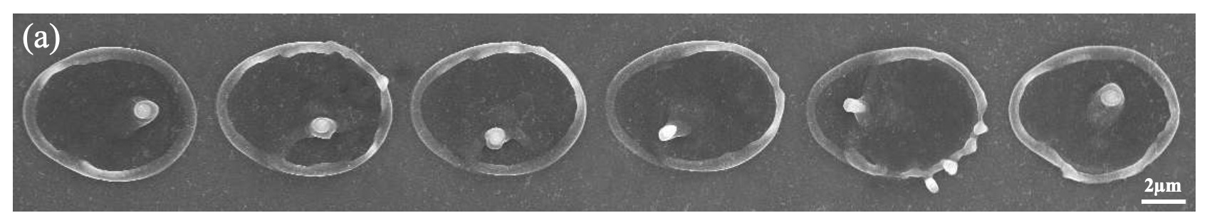
The ever-increasing demand for high data storage capacity has spurred research on innovative optical technologies that can transform the conventional GBytes optical discs (DVDs and Bluray) into ultrahigh capacity storage media. By encoding multi-level and multiplexed information in a localized volume within the recording medium TBytes storage capacities are feasible using different approaches. However, in almost all cases the recording medium had to be photosensitive, which required doping with photochromic molecules or nanoparticles in a multilayer stack or in the bulk material. Recently we observed that polymers that generally do not fluoresce will emit fluorescence in the visible spectrum when irradiated by a fs laser. This enables us to store data in common plastics without any special material preparation. Using a fs laser we were able to record grey level images by creating micron-sized modified regions representing bits in 3D. Upon excitation by a read laser, each modified region emits fluorescence whose intensity represented 8 grey levels; corresponding to 3 bits. We can currently achieve a storage capacity of 40 GB in a DVD size disc. We propose to extend this promising technique to further enhance the storage capacity to ~ 1TB/disc by increasing the number of grey levels and the packing density by reducing the bit size and spacing.

Embedded photonic devices
-
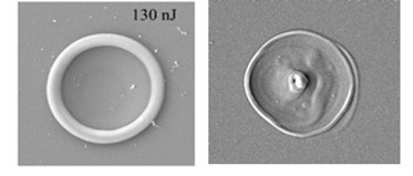
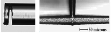
Using fs lasers, we can fabricate: (i) permanent waveguides and nano-gratings in 3D in glass by modifying refractive index, (ii) microfluidic channels by chemically etching the laser-modified regions, and (iii) nano-/micro-wells and grooves by laser ablation. These unique capabilities open new vistas for the development of novel photonic devices. We have recently demonstrated an in-line fiber cantilever vibration sensor and a narrow linewidth, low frequency noise random fiber laser. Fabricating 3D nano-gratings in the fiber core/cladding introduces anisotropic form birefringence making the medium polarization sensitive. Development of in-fiber polarization sensitive devices (polarizers and waveplates) minimizes the insertion losses and eliminate alignment issues. Ultrafast technology can also be used to develop novel fiber based biochemical sensors.
Laser processing of nanocomposites
-
Nano-composite materials (carbon and glass fiber reinforced plastics, multi-layered metal matrix) are widely used in the aerospace, sports and automotive industries. The interest in such materials is to exploit their unique physical properties such as lightweight, high stiffness and design flexibility in order to improve energy efficiency. Conventional techniques cause delamination, fiber frailing and thermal damage to the matrix that can induce micro-cracks and alter the material properties leading to catastrophic failure similar to the Columbia space shuttle. The use of short pulse lasers as a wear-free, ‘cold processing’ technology has very high potential and is believed to be the key technology for industrial production of nanocomposite components. Currently, very little research is conducted on ultrafast laser machining of composite materials. We address some of the challenges by testing and optimizing processes that lead to defect-free processing of composites and other emerging ‘difficult to machine’ materials.
Controlling interfacial properties
-
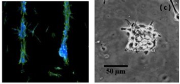
Altering the material properties at an interface has wide ranging applications from catalysis and bio-chemical sensing to tissue engineering and biomedical applications. One of the key challenges with biomaterials is enhanced cell adhesion and patterned growth (example, implant union). Often, cell adhesion is strongly influenced by physicochemical properties of substrates. A variety of techniques are used to change the surface properties of a material by altering the surface topography and/or chemistry. One such widely used technique is attaching the cell recognition motif RGD to the material via functional groups on the surface, but it is complex and involves multiple steps. Fs laser can be a promising one-step alternative to achieve patterned cell growth by altering the chemical (increased oxygen content) and wetting properties. Such control enables active guiding of cell growth in 3D, by incorporating microfluidic channels, for promoting cell infiltration and differentiation in spatially controlled volumes. Such structures in an implant enable faster regeneration and repair. We also investigate super-hydrophobicity induced by laser structuring of material surfaces.
Plastic electronics
-
Optical and electrical components can be integrated onto a single chip in silicon but the technology is planar. While 3D optical circuits can be fabricated in glass they are not suitable for electronic circuitry. This impasse can be overcome in polymers. Recently, we demonstrated formation of localized carbonaceous clusters in polymers irradiated with a fs laser. Electron hopping is known to occur among clusters leading to conductivity. Thus, electrical wiring and optical circuitry are feasible with a fs laser. In this project we explore the laser parameters to control the cluster size and density and thereby optimize conductivity.
Direct laser lithography
-
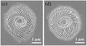
Engineering material properties is key for development of smart materials and next generation nanodevices. This requires nanoscale spatial precision and control to fabricate structures/defects. Sub-wavelength structuring of materials enables to alter the material properties (optical, electrical, mechanical and chemical) with applications in areas such as plasmonics, sensing, catalysis, wettability and light control. It is driven by the ever-increasing demand for miniaturization and integrated optics. While lithographic techniques are widely used for nanostructuring, direct mask-less fabrication is only possible with electron and ion beams. Light has an inherent disadvantage; diffraction imposes a fundamental limit to spatial resolution of any optical system. Diffraction also dictates how tightly a laser beam can be focused, which in turn determines the feature size one can achieve in laser ablation/modification of materials.
-
We are exploring different techniques to produce and spatially control sub-diffraction limited structures. First, multi-color machining vis-à-vis seeded avalanching – shorter wavelengths to localize the seed electrons and intense longer wavelengths to induce the ablation/modification process. Second, structured light beams to control the intensity and phase distribution. Third, use XUV light produced by high harmonic generation because achievable feature size that scales with wavelength.