MOCVD:
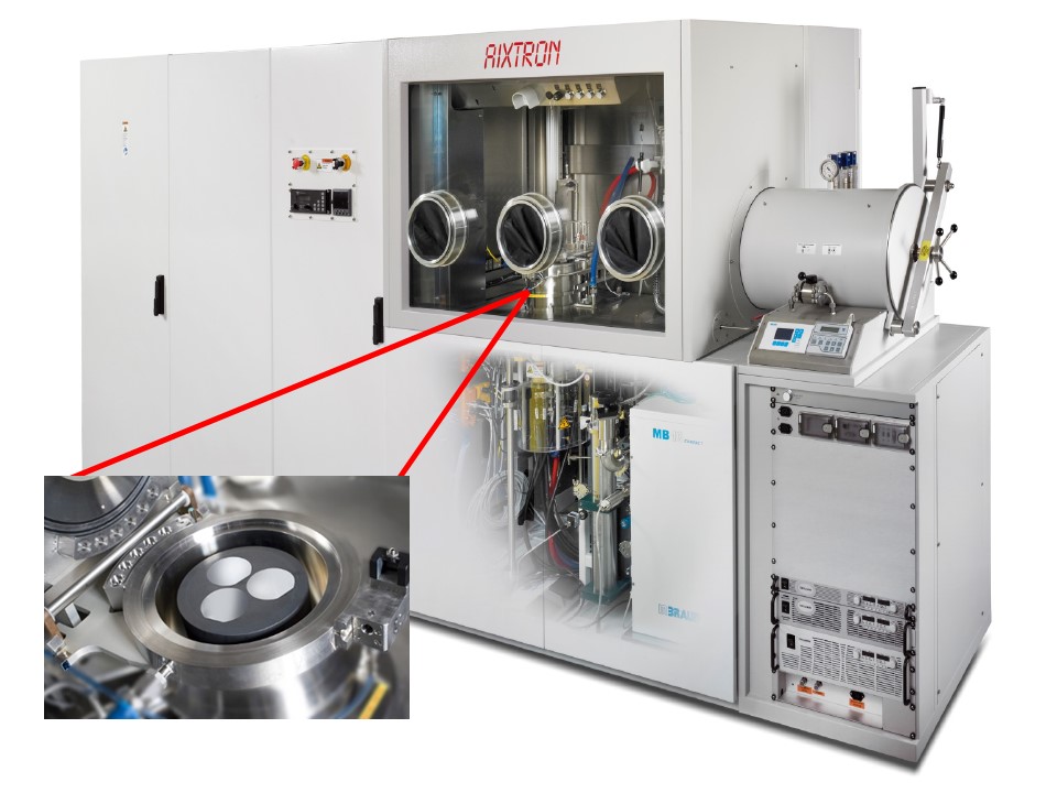
We have established an epitaxy laboratory for the growth of 2-dimensional materials including graphene, hexagonal boron nitride, and transition-metal dichalcogenides (WS2, MoS2, WSe2, MoSe2, etc.). Our MOCVD system allows for the simultaneous growth on three 2-inch diameter substrates which may be sapphire, silicon or wafers with additional dielectric coatings or patterning.
The ability to grow 2D materials on the wafer scale represents a paradigm shift in the development of 2D circuits and the evolution towards commercialization and manufacturability. We can now contemplate and plan for the design of full-wafer device nanofabrication.
Beyond the growth of single 2D epitaxial layers, we are also focused on the growth of heterostructures – i.e. stacks of different 2D materials in a van der Waals configuration.
AFM Characterization:
One method of characterizing the growth of 2D materials is through the use of an atomic force microscope, AFM. The AFM is able to measure the topography of a sample using the attractive van der Waals force, it does this by lowering a tip very close to the sample, so that the tip is attracted towards the sample, bending the tip downwards. While this is happening a laser is projected onto the back of the tip, so when the tip bends towards the tip of the sample the laser reflection path is changed. The laser deflection position is measured by a position-sensitive detector. The system uses these data to create a image of the topography of the sample, as well as a 3D image of the surface features.
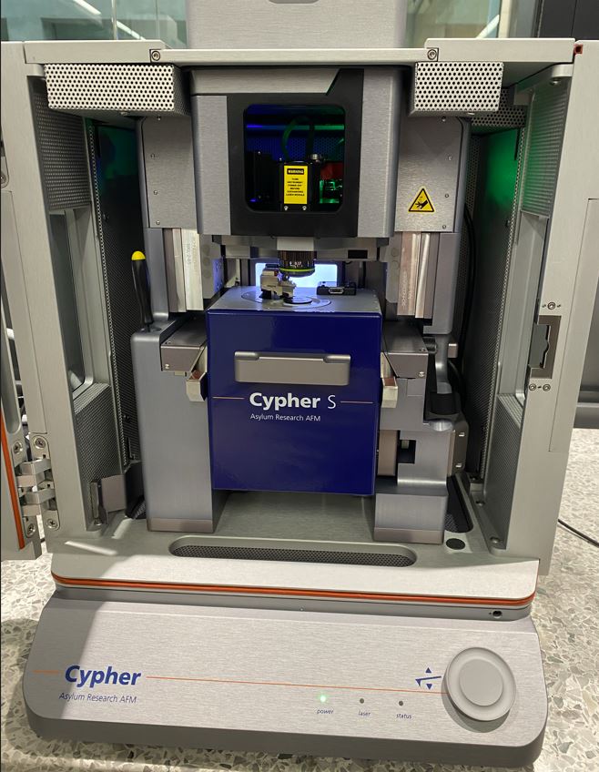
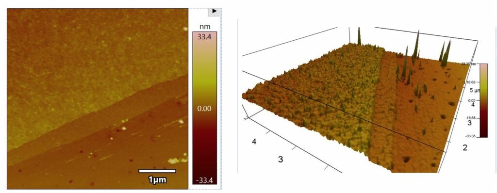
The specific AFM used in this lab is Asylum Research’s Cypher, primarily using the AC160 tip. Through this AFM we have been able to image sample of Graphene on a sapphire substrate and hBN on a sapphire substrate. These images allow us to see the surface features of the sample on a nanometer scale, features which often can’t be seen trough an optical microscope.
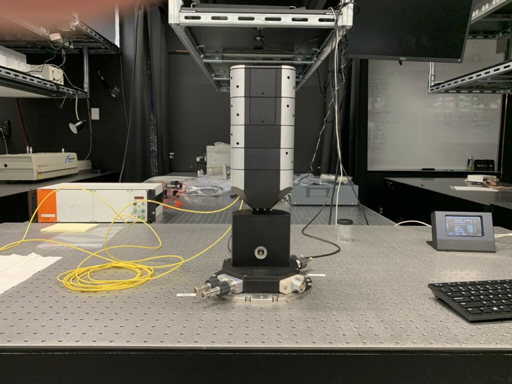
The Image on the left portrays the Cypher AFM, the sample fits one the top of the blue box in the center. The tip holder can also be seen, being the piece on top of the blue box, that over hangs where the sample is placed. Above the tip and sample is an optical microscope that is used to position the tip in specific spots on the sample. Finally above the optical microscope is the laser detector that is used to detect the deflection of the tip as it moves across the sample.
After the AFM has taken the image we are able to assign a colour set to it, as it is not taken an optical image just a set of pixel heights, most commonly we use the colour set number2. Often with the images they are not always flat and will have a slight tilt to the surface, to remove this a planefit is applied to the image to give it the flat surface.
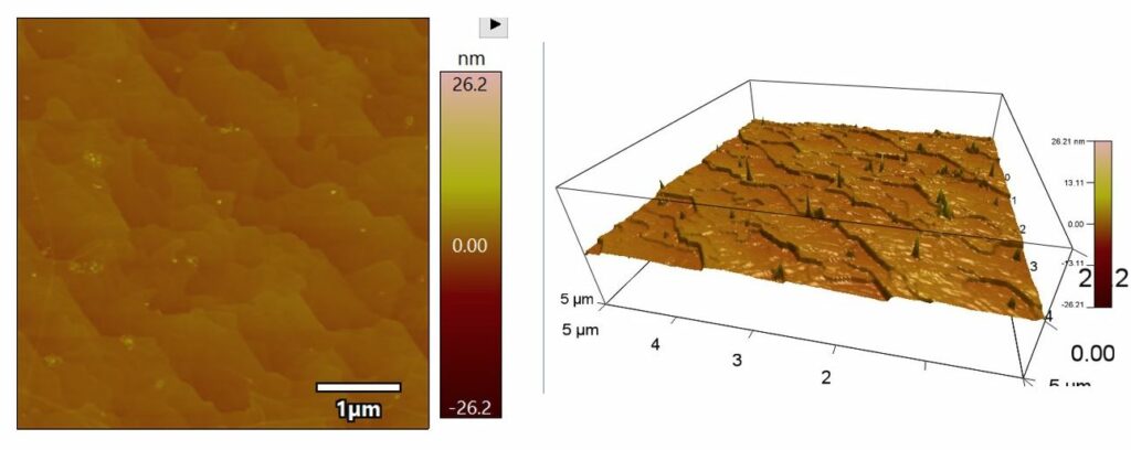
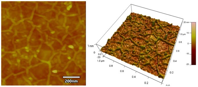
A 2D image of the topography of hBN, as well as the 3D image of the surface.
These scans give us important information such as surface feature height and growth patterns.
Attocube:
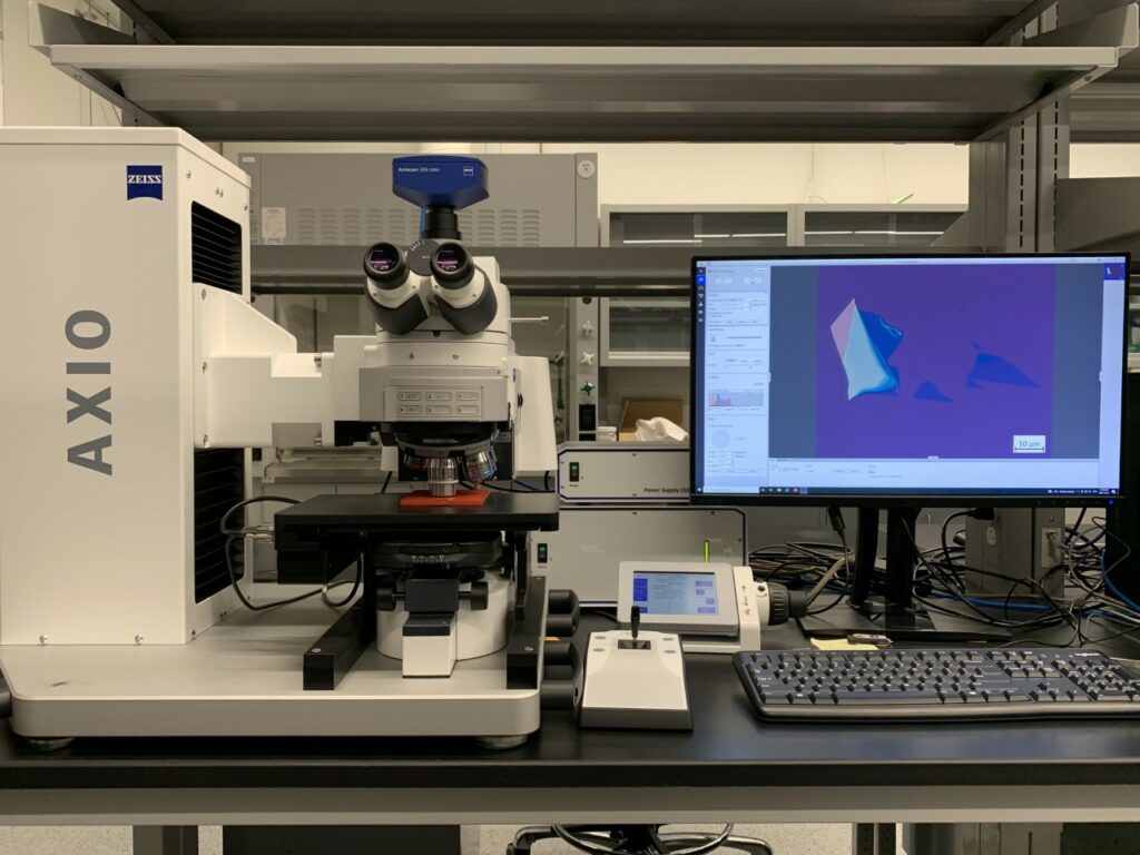
Optical Microscopy