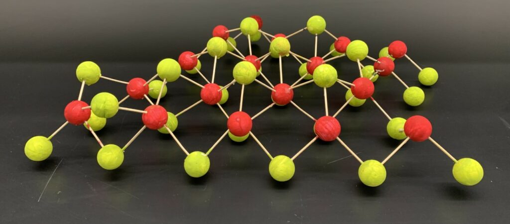
We are focussed on the development of ultrahigh quality single-crystal 2D materials (graphene, hexagonal boron nitride and transition-metal dichalcogenides) for electronic and optoelectronic applications.
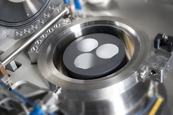
A key feature of this work is the wafer-scale growth of these materials using a commercial Aixtron close-coupled showerhead MOCVD system. This allows us to produce uniform 2D films and heterostructures on a fab-ready scale using 3X50mm, 1X76mm or 1X100mm semiconductor wafers.
We have also built a dedicated characterization laboratory featuring a suite of state-of-the-art physical and spectroscopic instruments. These characterization methods include high-resolution confocal photoluminescence and Raman mapping; optical microscopy with differential interference contrast; and atomic force microscopy (AFM). More information about these specific characterization methods can be found in the research section.
The 2D-MOCVD and characterization labs are both located in the University of Ottawa’s new STEM building.
Opportunities are available for talented undergraduate and graduate students: Graduate Student Opportunities to begin in Jan., May or Sept. 2024. Please contact Professor Gupta for more information.
Contact Information
- Dr. James Gupta
- Email: jgupta4@uottawa.ca
- Office Number: STM 443